
Shaping the Future: Key Semiconductor Trends in Computing & Data Infrastructure
PLUS: Former Bytedance Engineering Lead Building Scalable Embedded DB for Object Storage

Behind The Scenes
Semiconductors have quietly powered nearly every technological breakthrough last year, enabling advancements in everything from AI-generated invitations to autonomous Waymo rides and edge computing. In 2024, innovations in high-performance computing, customized chip architectures, and intelligent workload distribution have pushed the boundaries of what’s possible across industries, laying the groundwork for a more interconnected and intelligent world.
In the realm of advanced materials, graphene, gallium nitride (GaN), and silicon carbide (SiC) have significantly improved chip performance and efficiency. Cutting-edge fabrication techniques - such as Arieca’s liquid metal elastomers - have not only reduced node sizes but also addressed critical heat dissipation challenges. Meanwhile, chipmakers have extended their innovation beyond silicon, transforming infrastructure itself. A notable example is Fungible Systems (now part of Microsoft), which leverages disaggregated systems to accelerate data-centric workloads in data centers.
Among the most exciting areas of innovation are:
High-performance computing
Customization and modularization
Intelligent compute placement
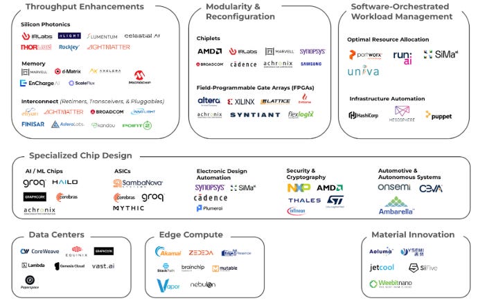
1) Advancements in High-Performance Computing (HPC)
High-performance computing (HPC) drives faster processing, optimized resource utilization, and scalable infrastructure. Innovation occurs at multiple levels - within individual chips, between racks, and through the interconnections that link these components.
Scale-up technologies focus on maximizing computational efficiency within a single rack by improving interconnections, memory access, and integration. These advancements enable faster data transfer and processing over short distances, leading to more efficient operations.
Silicon Photonics: This technology enables data transmission at nearly the speed of light, reducing latency and dramatically increasing bandwidth. Photonic Integrated Circuits (PICs) integrate optical components - such as lasers, waveguides, and modulators - onto a single chip. Unlike traditional electronic circuits that use electrons, PICs leverage photons for data transmission, resulting in lower latency and reduced power consumption. This innovation is particularly transformative for bandwidth-intensive applications like AI and machine learning.
Memory Stacking: Advances in stacked memory architectures allow for the integration of DRAM and SRAM directly onto boards, enabling faster data access while minimizing physical footprint. This approach is crucial for memory-intensive HPC workloads, ensuring efficient processing of large datasets.
Chiplets: Rather than relying on a single monolithic chip, chiplet technology integrates multiple smaller chip components into a cohesive package. Utilizing high-speed interconnects and silicon bridges, chiplets enhance scalability and functionality while overcoming the physical limitations of traditional chip designs.
(This article was written by Ayla Jeiroudi from Lotus Capital. For full version of this article, you can read them here.)
Geeks of the Week
Startup Name: Tonbo IO
Geography: China
One-liner: Tonbo develops edge-first data storage and analytics infrastructure.
Founder(s) Background: Team Lead (Time-Series DB Ingress team) at Bytedance,
Startup Name: Pacifica
Geography: US / Hong Kong
One-liner: Building the next generation of decentralized trading experience on Pacifica's own infrastructure.
Founder(s) Background: Co-CEO of FTX Digital Markets.
Startup Name: CurieTech AI
Geography: US
One-liner: AI-coding for IT Integrations.
Founder(s) Background: GM of AWS AI/ML services.
Founder(s) building in stealth
This edition is brought to you in partnership with Stella Capital.